VERIFICATION
Methodology
We at Chipout take pride in having our proven methodology for industry-leading tools in terms of RAL, SV/UVM TB generation and VIP Integration, GLS flows etc. With a holistic understanding of user requirements and by implementing the methodology, our team establishes a foundation for a robust Testbench architecture. This architecture encompasses stimulus generation, coverage tracking, and assertion-based verification.
Chipout has worked with multiple customers on small to very large designs taking full ownership of the verification closure. With well-defined verification flow, supported by the right methodologies and tools, significantly increases the likelihood of first-time success for our customers.
Tools & Technology
In the design verification phase, a suite of tools and software is instrumental in ensuring the accuracy and reliability of the ASIC design. This phase is highly dependent on tools provided by key suppliers such as Synopsys, Cadence, and Mentor. Our team is well-versed in utilizing tools from each supplier, enabling seamless integration across various verification methodologies.
Capabilities
Our Design Verification team excels in every facet of ASIC verification, ensuring the robustness and functionality of designs.
We have expertise in the following facets:
Verification Plan and Test Plan Development
Testbench Architecture Development
Test Case Writing and Debugging
Advanced Verification Techniques
Coverage and Regression Testing
Gate Level Simulation (GLS)
Version Control and Bug Reporting
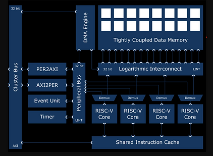
Multi-core RISC V / ARM / Power PC/ ATOM Processor-based Verification
High-Speed Protocol Verification
Formal Verification
Property proving/Proof kit development
We specialize in delivering solutions to our clients in domains like Compute, Mobile / Consumer, HPC, Networking and Automotive.

PHYSICAL DESIGN
Methodology
The field of ASIC Design is dynamic and full of challenges. The primary obstacle in dealing with these persistent challenges is the high cost involved in designing, verifying, and fabricating, coupled with tight deadlines, intense competition, and the complexity of product design and verification.
As technology advances and scales down from a higher node, like 28 nm, to a lower one, such as 2nm, the complexity of the process intensifies. Following Moore’s law, the number of transistors in a densely integrated circuit doubles approximately every two years, driven by the quest for increased computational power and capacity.
To tackle these challenges effectively, a proper methodology, along with the right tools and workflows, is essential. The journey of ASIC begins with understanding user requirements (specification) and progresses towards fabrication (Tape out). This journey can be lengthy, involving numerous critical tasks. Any failure in these tasks leads to chip failure, and even a re-spin of the chip is a costly endeavor that can impact business continuity. Therefore, a well-defined flow is necessary to ensure first-time success from specification to tape-out.
Tools & Technology
In the back-end design phase, various tools and software are utilized. This phase is very tools-centric with tools being provided by 3 key suppliers in Synopsys, Cadence and Mentor.
Our team is highly proficient in using these tools and in implementing the methodology flows across each of these tool vendors.
We bring in the expertise in the enlisted tools mentioned below:
Cadence (Cadence Innovus, Cadence Voltus IC Power Integrity Solution, Cadence Tempus Timing Signoff Solution)
Synopsys (Design Compiler, IC Compiler II, IC Validator, PrimeTime, PrimePower, PrimeRail)
Mentor (Caliber)
Our Team has Comprehensive physical design expertise for block and SoC designs spanning technology nodes from 28nm to 2nm from all fabs (TSMC, Intel and Samsung).
Capabilities
Chipout works with the world’s best fab and fab-less semiconductor companies which are working on the latest and greatest tech nodes.
At Chipout, the Physical design team has expertise on the latest and greatest 2nm Samsung technology and currently working on one of their low-power design. having multiple power and clock domains, complex logic with intensive macro partitions and abutted partition flows.
We specialize in implementing cutting-edge low-power techniques, such as clock gating, power gating, multi-Vt, and voltage islands, optimizing power efficiency for one of the world’s largest CPU/GPU/AI processor chip manufacturers.
Having a specialization in wireless and CDMA technologies, we have successfully delivered multiple projects for mobile processor chip manufacturer in 3nm/5nm/7nm to 28 nm technologies.

RTL Design
Our team has extensive and in-depth demonstrable expertise in several facets of the RTL / SoC design in the areas of networking, processor, multimedia, mobile, and automotive sectors.
Our specialists with decades of hands-on experience, an internally developed IP portfolio, and detailed exposure to TFM (Tools, flows, and methodologies) across the industry, enable our customers to a faster and more predictable time to market (TTM) and quality deliverables. The in-house processes which are in line with most of the industry standard practices, make Chipout one of the unique providers of RTL design solutions provider for the semiconductor industry.
Our team is capable of putting together system requirements, architecture definition, micro-architecture spec, RTL design, sanity test, various tool collateral creations, design checks and compliance using industry-standard tools and handing over the collaterals to the various stakeholders in Verification, DFT, and Physical implementation teams. The capability is not only restricted to IP design but also extends to subsystem or SoC design and integration. The Chipout team having worked with multiple Tier 1 customers, has great exposure to many complex projects and flows in UPF creation, static checks, design for PPA and trade-offs, DFT and DFV requirements.
Tools & Technology
In the RTL design phase, Industry standard tools are utilized ie. Synopsys, Cadence and Mentor. We have exposure to these tools and methodology flows.
Cadence: Xcelium, Genus, Tempus, Jasper, Conformal
Synopsys: VCS, Design Compiler, Formality, VCLP, Spyglass
Mentor: Questasim.
Capabilities
Architecture and Micro-architecture design for IP as well as SoCs
IP/SoC Design and Netlist delivery
Front-end design of complex multi-clock, power domain blocks, and low-power designs
RTL Signoff checks in Lint/, CDC (Clock domain crossing), FEC (Formal Equivalence Checks), Synthesis (logical/physical aware)
RTL design team has done and is capable of developing IPs like:
Slow peripheral like I2C, UART, SPI, SM Bus, PM Bus.
Fast Peripherals like PCIe, Ethernet, USB, etc
Infrastructure components in GPIO, Bus Bridges, SoC interconnect, Subsystem / SoC bus architectures, AMBA Bus Interfaces like APB, AHB, AXI
CPU Design – RISC-V, Power PC, ARM CPUs, Cache Controllers, MMU, IO-Coherency, Fast ALUs, MACs and Multi-core Coherent CPU Subsystems
DSP IPs like FFT, FM Modulator Clock, and Reset generators for SoC / Subsystems Low power design, SoC integration


